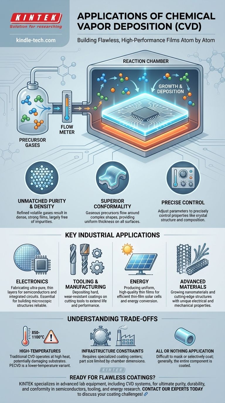
At its core, Chemical Vapor Deposition (CVD) is a highly versatile manufacturing process used to create exceptionally high-purity and high-performance thin films and coatings. Its primary applications are in the electronics industry for fabricating semiconductor devices, on cutting tools to create wear-resistant surfaces, and in the energy sector for producing thin-film solar cells.
The true value of CVD lies not just in applying a coating, but in its ability to grow a new, dense, and perfectly uniform solid layer on a substrate, atom by atom. This makes it the essential choice for applications where the quality and conformity of the film are absolutely critical to performance.
The Principle: Building Materials from Gas
Chemical Vapor Deposition is fundamentally different from painting or spraying. It involves introducing precursor gases into a reaction chamber where they decompose and react on the surface of a heated substrate, meticulously building the desired film.
Unmatched Purity and Density
Because the source materials are volatile gases, they can be refined to incredibly high levels of purity. This process results in solid films that are dense, strong, and largely free of the impurities that can plague other coating methods.
Superior Conformality
The gaseous precursors flow around the substrate, depositing a film of uniform thickness on all surfaces, including complex shapes and internal cavities. This "wrap-around" capability is a significant advantage over line-of-sight deposition techniques.
Precise Control Over Properties
By carefully adjusting deposition parameters like temperature, pressure, and gas composition, engineers can precisely control the final film's characteristics. This includes its crystal structure, chemical composition, and grain size.
Key Industrial Applications Explained
The unique characteristics of CVD make it indispensable in several high-technology fields. Its application is dictated by the need for performance that less advanced methods cannot achieve.
The Foundation of Modern Electronics
The fabrication of integrated circuits involves depositing dozens of ultra-thin layers of conducting, semiconducting, and insulating materials. CVD provides the purity and precise thickness control required to build these microscopic structures reliably.
Enhancing Durability and Performance
Hard ceramic coatings are deposited via CVD onto industrial cutting tools, drills, and machine components. These dense, low-stress films dramatically increase resistance to wear, corrosion, and high temperatures, extending the life and performance of the tools.
Powering a Sustainable Future
CVD is used to deposit the thin layers of photovoltaic materials that form the active region of thin-film solar cells. The high quality and uniformity of these films are essential for efficiently converting sunlight into electricity.
Advanced Materials and Nanotechnology
The process is also critical in cutting-edge research and manufacturing. It is a preferred method for growing advanced materials like carbon nanotubes and various nanowires, which have unique electrical and mechanical properties.
Understanding the Practical Trade-offs
Despite its advantages, CVD is not a universal solution. Its operational requirements introduce specific limitations that must be considered.
High-Temperature Requirements
Traditional CVD processes operate at very high temperatures, often between 850-1100°C. This heat can damage or warp many substrate materials, limiting its use. However, variants like Plasma-Enhanced CVD (PECVD) can operate at much lower temperatures to overcome this.
Process and Infrastructure Constraints
CVD is not a portable process; parts must be sent to a specialized coating center. The size of the components that can be coated is limited by the dimensions of the vacuum chamber, and complex assemblies must be broken down into individual parts before treatment.
The "All or Nothing" Application
The nature of the process makes it very difficult to mask or selectively coat only a portion of a surface. Generally, the entire component exposed within the chamber will be coated.
Making the Right Choice for Your Goal
Selecting the right coating technology depends entirely on your end goal. CVD excels where ultimate performance is the primary driver.
- If your primary focus is maximum purity and film quality: CVD is the superior choice for applications like semiconductors or high-performance optics where material integrity is non-negotiable.
- If your primary focus is enhancing durability on complex shapes: CVD's excellent "wrap-around" capability makes it ideal for uniformly coating intricate components like engine parts or specialized tools.
- If your primary focus is coating temperature-sensitive materials: Standard CVD is unsuitable; you must explore lower-temperature variants like Plasma-Enhanced CVD (PECVD) to avoid damaging your substrate.
Ultimately, Chemical Vapor Deposition is the definitive technology for creating flawless, high-performance films that become an integral part of the underlying material.
Summary Table:
| Application Area | Key Use of CVD |
|---|---|
| Electronics | Fabricating ultra-pure, thin layers for semiconductors and integrated circuits. |
| Tooling & Manufacturing | Depositing hard, wear-resistant coatings on cutting tools and components. |
| Energy | Producing uniform, high-quality thin films for solar cells. |
| Advanced Materials | Growing nanomaterials like carbon nanotubes and nanowires. |
Ready to integrate flawless, high-performance coatings into your products?
KINTEK specializes in advanced lab equipment, including Chemical Vapor Deposition systems, to help you achieve the ultimate in film purity, durability, and conformity for your most critical applications in semiconductors, tooling, and energy research.
Contact our experts today to discuss how CVD technology can solve your specific coating challenges!
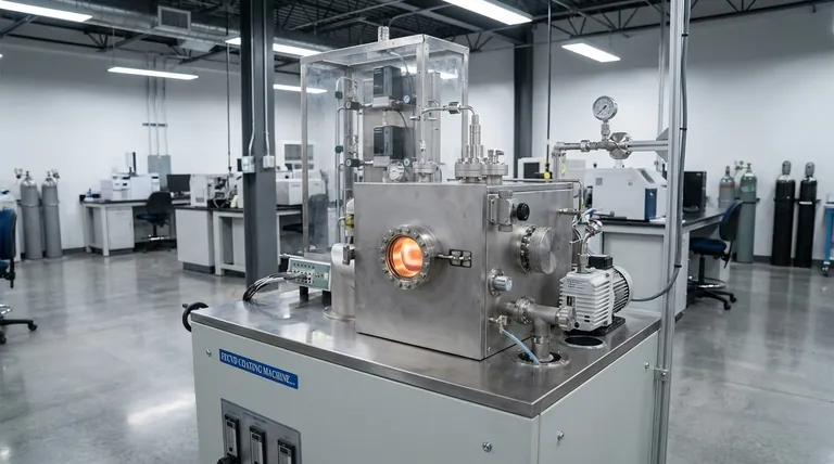
Visual Guide
Related Products
- Chemical Vapor Deposition CVD Equipment System Chamber Slide PECVD Tube Furnace with Liquid Gasifier PECVD Machine
- RF PECVD System Radio Frequency Plasma-Enhanced Chemical Vapor Deposition RF PECVD
- Microwave Plasma Chemical Vapor Deposition MPCVD Machine System Reactor for Lab and Diamond Growth
- Customer Made Versatile CVD Tube Furnace Chemical Vapor Deposition Chamber System Equipment
- 915MHz MPCVD Diamond Machine Microwave Plasma Chemical Vapor Deposition System Reactor
People Also Ask
- What is plasma enhanced chemical vapor deposition PECVD equipment? A Guide to Low-Temperature Thin Film Deposition
- How expensive is chemical vapor deposition? Understanding the True Cost of High-Performance Coating
- Why is Chemical Vapor Deposition (CVD) equipment uniquely suited for constructing hierarchical superhydrophobic structures?
- What is the chemical vapor deposition growth process? Build Superior Thin Films from the Atom Up
- What are the advantages of chemical vapor deposition? Achieve Superior Thin Films for Your Lab


