At its core, Metal Organic Chemical Vapor Deposition (MOCVD) is a highly controlled process for creating ultra-pure, crystalline thin films. It involves introducing specific volatile metal-organic precursor gases into a reaction chamber where they decompose on a heated substrate, chemically reacting to form a solid material layer by layer. This method offers exceptional control over thickness, composition, and crystal structure.
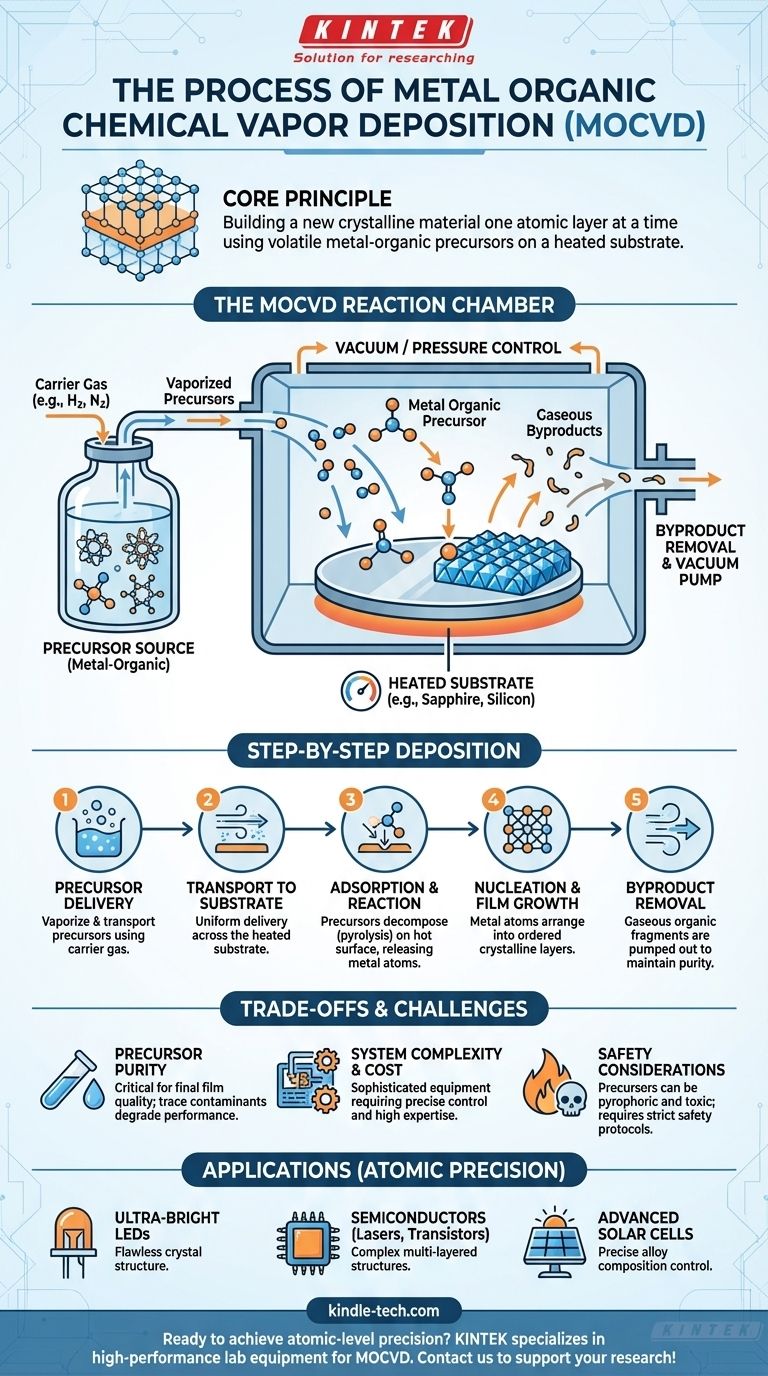
The central principle of MOCVD is not merely coating a surface, but rather building a new crystalline material one atomic layer at a time. This is achieved by using carefully designed precursor molecules that controllably break apart at a specific temperature, depositing their metallic atoms onto a substrate with extreme precision.
The Key Components of the MOCVD Process
To understand the MOCVD process, you must first understand its three primary components: the precursors, the substrate, and the reaction chamber. Each plays a critical role in the final quality of the film.
What Makes a "Metal Organic" Precursor Special?
A metal organic precursor is a complex molecule where a central metal atom is bonded to organic molecules (ligands). These precursors are engineered to have very specific properties.
They must be volatile, meaning they can be easily turned into a gas and transported into the reaction chamber. Crucially, they are also designed to decompose cleanly at a precise temperature, releasing the desired metal atom onto the substrate surface while the organic components become waste byproducts that are easily removed.
The Substrate: A Template for Growth
The substrate is not a passive component; it is the foundation upon which the new material is built. It is typically a crystalline wafer (like sapphire or silicon) that is heated to a precise temperature.
This heat provides the thermal energy required to break the chemical bonds in the precursor molecules. The substrate's own crystal structure acts as a template, guiding the deposited atoms to arrange themselves into an ordered, crystalline film in a process known as epitaxial growth.
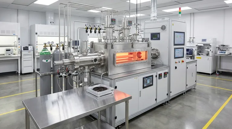
The Reaction Chamber: A Controlled Environment
The entire process takes place within a reaction chamber under a controlled vacuum or specific pressure. This environment is critical for two reasons.
First, it ensures purity by removing any unwanted molecules that could contaminate the film. Second, it allows for precise control over the flow of precursor and carrier gases, directly influencing the growth rate and composition of the final material.
A Step-by-Step Breakdown of Deposition
The MOCVD process can be broken down into a series of distinct, sequential steps that transform gaseous chemicals into a solid, high-performance film.
Step 1: Precursor Delivery
The metal organic precursors, which are often liquids or solids at room temperature, are vaporized. A carrier gas (like hydrogen or nitrogen) is bubbled through or passed over the precursors, picking them up and transporting them in gaseous form into the reaction chamber.
Step 2: Transport to the Substrate
Inside the chamber, a carefully managed flow of gases moves across the heated substrate. The physics of this gas flow is critical for ensuring that the precursor molecules are delivered uniformly across the entire surface of the substrate.
Step 3: Adsorption and Surface Reaction
When the precursor molecules strike the hot substrate, they "adsorb," or stick, to the surface. The thermal energy from the substrate causes them to decompose (pyrolysis). The bonds holding the metal atom to its organic ligands break apart.
Step 4: Nucleation and Film Growth
The freed metal atoms are now mobile on the substrate surface. They diffuse across the surface until they find an energetically favorable site, often dictated by the underlying crystal structure of the substrate. Here, they bond together, forming the first atomic layer of the new crystalline film. This process repeats, building the film layer by layer.
Step 5: Desorption and Byproduct Removal
The leftover organic fragments from the decomposed precursors are now gaseous waste products. These byproducts, along with any unreacted precursors, desorb from the surface and are transported away by the carrier gas, eventually being pumped out of the chamber.
Understanding the Trade-offs and Challenges
While incredibly powerful, MOCVD is a complex and demanding technique with significant trade-offs that must be considered.
The Challenge of Precursor Purity
The quality of the final crystalline film is directly dependent on the purity of the precursor chemicals. Even trace amounts of contaminants can disrupt the crystal structure and degrade the material's performance. Sourcing and handling these ultra-pure chemicals is a major cost and logistical challenge.
System Complexity and Cost
MOCVD reactors are sophisticated and expensive pieces of equipment. They require precise control over temperature, pressure, and gas flow, all managed within a high-vacuum environment. Operating and maintaining these systems demands significant expertise and investment.
Critical Safety Considerations
Many of the metal organic precursors used in MOCVD are pyrophoric (ignite spontaneously in air) and highly toxic. This necessitates strict and complex safety protocols for storage, handling, and disposal, adding another layer of operational complexity.
Applying MOCVD to Your Goal
The decision to use MOCVD is driven entirely by the need for crystalline quality and compositional control that other methods cannot provide.
- If your primary focus is atomic-level precision: MOCVD is the industry standard for creating complex, multi-layered semiconductor structures for devices like high-performance lasers and transistors.
- If your primary focus is high-quality crystalline growth: MOCVD is essential for fabricating materials where flawless crystal structure is paramount to performance, such as in the manufacturing of ultra-bright LEDs.
- If your primary focus is compositional control: MOCVD allows for the precise mixing of different precursors to create specific alloy compositions, enabling the production of advanced solar cells and other optoelectronic devices.
Ultimately, MOCVD is the foundational process that enables much of modern high-technology by giving us the ability to engineer materials at the atomic scale.
Summary Table:
| MOCVD Process Stage | Key Action | Purpose |
|---|---|---|
| Precursor Delivery | Vaporize metal-organic compounds | Create gaseous reactants for transport |
| Transport to Substrate | Flow gases across heated substrate | Ensure uniform precursor distribution |
| Adsorption & Reaction | Precursors decompose on hot surface | Release metal atoms for deposition |
| Nucleation & Growth | Atoms form crystalline layers | Build material with precise structure |
| Byproduct Removal | Pump out organic fragments | Maintain purity and process control |
Ready to achieve atomic-level precision in your lab? KINTEK specializes in high-performance lab equipment and consumables for advanced deposition processes like MOCVD. Our solutions help laboratories fabricate superior LEDs, semiconductor devices, and optoelectronic materials with exceptional crystalline quality and compositional control. Contact our experts today to discuss how we can support your thin-film research and production goals!
Visual Guide
Related Products
- 915MHz MPCVD Diamond Machine Microwave Plasma Chemical Vapor Deposition System Reactor
- Multi Heating Zones CVD Tube Furnace Machine Chemical Vapor Deposition Chamber System Equipment
- Microwave Plasma Chemical Vapor Deposition MPCVD Machine System Reactor for Lab and Diamond Growth
- Cylindrical Resonator MPCVD Machine System Reactor for Microwave Plasma Chemical Vapor Deposition and Lab Diamond Growth
- Customer Made Versatile CVD Tube Furnace Chemical Vapor Deposition Chamber System Equipment
People Also Ask
- How do vacuum pumps and valves collaborate in MPCVD? Achieve Precise Pressure Control for Superior CNT Synthesis
- What is the CVD process of diamond? How Lab-Grown Diamonds Are Created
- Why is MW-CVD preferred for high-purity diamond optical windows? Achieve Zero-Contamination Material Growth
- What are the primary advantages of the CVD method for growing diamonds? Engineering High-Purity Gems and Components
- How are CVD diamonds created? Discover the Science of Lab-Grown Diamond Precision


