All Questions
What Are The Different Techniques For Carbon Nanotube Synthesis? From Research To Industrial Scale
Explore the primary carbon nanotube synthesis methods: arc discharge, laser ablation, and chemical vapor deposition (CVD), and learn which is best for your needs.
What Is The Catalyst For The Growth Of Carbon Nanotubes? From Metal Nanoparticles To Market Demand
Explore the dual catalysts for CNT growth: scientific (Fe, Co, Ni nanoparticles) and market (lithium-ion batteries). Understand synthesis, challenges, and applications.
Is It Possible During The Synthesis Of Cnts To Determine Its Chirality? Master The Challenge Of Cnt Purity Control
Explore the feasibility of controlling CNT chirality during synthesis, the challenges of scalable production, and practical solutions for achieving purity.
How Does Chirality Affect Carbon Nanotubes? It Determines If They Are Metal Or Semiconductor
Chirality, defined by the (n,m) vector, dictates if a carbon nanotube is a metallic conductor or a semiconductor, impacting all electronics applications.
What Is The Chirality Diameter Of A Carbon Nanotube? How Chirality Determines Cnt Properties
Learn how a carbon nanotube's (n,m) chirality dictates its exact diameter, electronic properties, and applications. Essential for nanotech R&D.
What Are The Techniques Of Carbon Nanotubes? Master Synthesis For Your Application
Explore the primary carbon nanotube synthesis techniques: arc discharge, laser ablation, and CVD. Learn how each method impacts quality, scalability, and cost.
Can Carbon Nanotubes Be Used As Catalyst Support? Yes, For Superior Catalytic Performance.
Discover why carbon nanotubes excel as catalyst supports due to high surface area, stability, and tunable electronic properties for enhanced reactions.
How Does Carbon Nanotubes Work? Unlocking Superior Strength And Conductivity For Your Lab
Discover how carbon nanotubes' unique structure provides exceptional electrical conductivity and mechanical strength for advanced applications in batteries and composites.
How Can Nanotubes Be Used As A Catalyst? Enhance Performance And Durability Of Metal Catalysts
Learn how carbon nanotubes act as superior catalyst supports, boosting efficiency, stability, and selectivity in chemical reactions through enhanced surface area and electronic interactions.
What Are The Future Uses Of Cnts? Revolutionizing Electronics, Energy, And Materials
Explore the future of Carbon Nanotubes (CNTs) in electronics, energy storage, and ultra-strong composites. Learn how CNTs are set to transform industries.
What Nanomaterials Are Synthesized By Chemical Vapor Deposition? Building High-Performance Materials With Precision
Explore how Chemical Vapor Deposition (CVD) synthesizes graphene, carbon nanotubes, and essential thin films for electronics and advanced materials.
What Are The Characterization Of Single-Walled Carbon Nanotubes? Essential Techniques For Swcnt Analysis
Learn key methods for characterizing SWCNTs: TEM for structure, Raman for quality, UV-Vis-NIR for electronic type, and PL for chirality mapping.
Which One Is A Characterization Technique In Carbon Nanotubes? Understand The Key Difference Between Making And Measuring
Learn the critical difference between carbon nanotube synthesis (e.g., CVD) and characterization (e.g., SEM, Raman) to ensure material quality and application success.
How Are Carbon Nanotubes Characterized? A Guide To Verifying Quality And Performance
Learn the key techniques—TEM, SEM, Raman, TGA, XPS—to characterize CNT structure, purity, and surface chemistry for your application.
Are Carbon Nanotubes Safe For The Environment? Weighing Performance Benefits Against Ecological Risks
Explore the environmental safety of carbon nanotubes (CNTs), including their lower CO2 footprint versus risks of toxicity and persistence in ecosystems.
What Are The Methods Of Carbon Nanotubes Fabrication? From Arc Discharge To Scalable Cvd
Explore the three main carbon nanotube fabrication methods: Arc Discharge, Laser Ablation, and Chemical Vapor Deposition (CVD), the industry standard for scalability.
What Are The Three Different Ways Of Synthesising Carbon Nanotubes? A Guide To Methods And Trade-Offs
Explore the three main methods for carbon nanotube synthesis: Arc Discharge, Laser Ablation, and Chemical Vapor Deposition (CVD), the commercial standard.
What Catalyst Is Used In Growing Carbon Nanotubes By Chemical Vapor Deposition? Key Metals For Controlled Synthesis
Discover the role of Fe, Co, and Ni catalysts in CNT growth via CVD. Learn how catalyst choice affects nanotube diameter, structure, and yield.
Why Carbon Nanotubes Are Used In Catalyst Systems? Enhance Efficiency With Superior Catalyst Support
Discover how carbon nanotubes (CNTs) boost catalyst performance with high surface area, excellent conductivity, and superior stability for demanding applications.
How Are Carbon Nanotubes Synthesized By Arc Discharge? The Original High-Temperature Method Explained
Learn how the arc discharge method synthesizes carbon nanotubes using high-temperature plasma, and understand its role in producing high-quality nanotubes.
What Are The Synthesis And Purification Methods For Carbon Nano Tubes? Scaling Quality And Purity For Your Application
Compare arc discharge, laser ablation, and CVD methods for carbon nanotube synthesis and the essential purification steps needed for high-performance materials.
What Are The Mechanical Applications Of Carbon Nanotubes? Reinforce Materials For Unmatched Strength
Explore how carbon nanotubes enhance mechanical properties in composites, concrete, and polymers for superior strength, durability, and performance.
What Are The Applications Of Carbon Nanomaterials? Unlock Revolutionary Performance In Energy, Materials & Electronics
Explore how carbon nanomaterials enhance batteries, composites, and sensors. Discover their key applications in energy, materials science, and electronics.
What Are The Useful Applications Of Carbon Nanotubes? Enhance Materials For Batteries, Composites, And Electronics
Discover how carbon nanotubes improve lithium-ion batteries, reinforce composites, and enable next-gen electronics with superior conductivity and strength.
Why Are Carbon Nanotubes Important In Industry? Unlocking Next-Generation Material Performance
Discover how carbon nanotubes (CNTs) enhance lithium-ion batteries, enable advanced composites, and drive innovation in electronics and energy storage.
What Can Carbon Nanotubes Be Used For? Unlock Superior Performance In Batteries & Materials
Carbon nanotubes enhance lithium-ion batteries, polymers, composites & more. Learn how CNTs add conductivity, strength & durability.
What Can Carbon Nanotubes Replace? Upgrade Your Materials With Superior Performance
Discover how carbon nanotubes replace carbon black and other additives for better conductivity, strength, and sustainability in batteries and composites.
Are Carbon Nanotubes Used In Industry? Unlocking High-Performance Materials
Explore how carbon nanotubes are used in industry today, from boosting lithium-ion battery performance to creating stronger, conductive composites.
What Are The Toxic Effects Of Carbon Nanotubes? Understanding The Risks Of Inhalation
Learn about carbon nanotube toxicity, from asbestos-like lung effects to safety measures for handling. Essential reading for lab professionals.
What Are The Environmental Applications Of Carbon Nanotubes? Boost Efficiency & Sustainability
Explore how carbon nanotubes enhance batteries, composites, and electronics for greater energy efficiency, reduced waste, and lower emissions.
Why Are Carbon Nanotubes Bad For The Environment? Understanding The Toxicity Vs. Performance Trade-Offs
Explore the environmental impact of carbon nanotubes (CNTs), including toxicity risks, ecotoxicity, and persistence, compared to alternatives like carbon black.
How Is Carbon Nanotubes Structured? From Graphene Sheets To 1D Cylinders
Explore the atomic structure of carbon nanotubes, from their graphene honeycomb lattice foundation to how chirality defines their metallic or semiconducting properties.
What Is Flame Synthesis Method For Carbon Nanotubes? Scalable, Low-Cost Production For Industrial Applications
Learn how flame synthesis uses combustion to produce carbon nanotubes continuously, offering industrial-scale output and lower costs compared to furnace methods.
What Is The Synthesis And Mechanism Involved In The Preparation Of Carbon Nanotubes Using Cvd Process? Master Controlled Growth For Your Application
Learn the step-by-step CVD mechanism for carbon nanotube synthesis, including catalyst preparation, carbon diffusion, and key parameters for controlling CNT properties.
What Are The Methods Of Synthesis For Carbon Nanotubes? A Guide To Arc Discharge, Laser Ablation & Cvd
Explore the three core methods for synthesizing carbon nanotubes: arc discharge, laser ablation, and Chemical Vapor Deposition (CVD). Learn which is best for your application.
What Are The Different Types Of Nanocarbons? A Guide To Fullerenes, Nanotubes, And Graphene
Explore the main types of nanocarbons: fullerenes, carbon nanotubes, and graphene. Learn how their structure defines their unique properties and applications.
What Are The Different Types Of Single-Walled Carbon Nanotubes? Armchair, Zigzag, And Chiral Structures Explained
Learn about the three types of SWCNTs—Armchair, Zigzag, and Chiral—and how their atomic structure determines metallic or semiconducting properties.
What Are Carbon Nanotubes Explain Its Types? Unlocking The Power Of Swcnts And Mwcnts
Learn about single-walled (SWCNT) and multi-walled (MWCNT) carbon nanotubes, their properties, and key applications in electronics and materials.
What Are The Categories Of Carbon Nanotubes? Understand Swcnt Vs. Mwcnt For Your Application
Learn the two main categories of carbon nanotubes (SWCNT vs. MWCNT) and how their structure (chirality) determines electrical and mechanical properties.
What Is The Capacity Of Carbon Nanotubes? Unlock Their Potential In Electronics, Energy, And Materials
Explore carbon nanotube capacities: from 10⁹ A/cm² current density to 100 GPa tensile strength. Learn how to apply CNTs in energy storage, electronics, and composites.
Why Is Mass Producing Carbon Nanotubes A Challenge Today? The Trilemma Of Scale, Quality, And Cost
Explore the core challenges in CNT mass production: the trade-off between volume, purity, and cost. Learn why control and uniformity remain key hurdles.
Can Carbon Nanotubes Be Mass Produced? Scaling Cnt Production For Commercial Applications
Learn how carbon nanotubes are mass-produced using CVD, the trade-offs in quality vs. quantity, and the future of industrial CNT manufacturing.
Are Carbon Nanotubes Hard To Make? Mastering The Challenge Of Scalable, High-Quality Production
Explore the complexities of carbon nanotube synthesis, from chirality control to purity challenges, and the trade-offs between quality and scalability.
What Are The Challenges In The Use Of Carbon Nanotubes For Biomedical Applications? Navigating Toxicity And Safety Hurdles
Explore the key challenges of carbon nanotubes in biomedicine, including toxicity, poor solubility, and long-term biodistribution concerns.
Are Carbon Nanotubes Stronger Than Graphene? Choosing The Right Carbon Nanomaterial For Your Application
Explore the strength of graphene vs. carbon nanotubes: theoretical limits vs. practical usability. Learn which material is right for your project.
What Is The Difference Between Graphene And Carbon? It's All About Atomic Structure
Graphene is a 2D allotrope of carbon. Learn how its unique honeycomb lattice structure creates extraordinary properties compared to other carbon forms.
Why Carbon Nanotubes Are Better Than Graphene? Matching Material Geometry To Your Engineering Challenge
Discover when carbon nanotubes excel over graphene due to their 1D structure for wiring, composites, and field emission, and when graphene's 2D properties are superior.
What Is The Difference Between Carbon Nanotubes And Graphene Oxide? Choose The Right Nanomaterial For Your Application
Understand the key differences between CNTs and graphene oxide: structure, conductivity, processability, and how to select the best material for your project.
What Are 2 Properties Of Carbon Nanotubes That Make It Special? Unmatched Strength & Conductivity
Discover the 2 key properties of carbon nanotubes: exceptional mechanical strength and unique electrical conductivity, enabling advanced materials and electronics.
What Are Carbon Nanotubes Advantages And Disadvantages? Balancing Performance And Practicality
Explore the pros and cons of carbon nanotubes (CNTs), including their unmatched strength and conductivity versus challenges like high cost and dispersion issues.
What Are The Advantages Of Carbon Nanotubes Over Steel? Unmatched Strength & Conductivity
Discover why carbon nanotubes offer superior strength-to-weight ratio and conductivity vs. steel, ideal for high-performance composites and electronics.
What Are The Advantages Of Carbon Nanotubes? Unlock Superior Strength, Conductivity & Performance
Discover the key advantages of carbon nanotubes (CNTs): exceptional strength, superior electrical & thermal conductivity, and their role in enhancing batteries & composites.
What Is A Potential Application For The Nanotubes? Boost Performance In Batteries, Composites & Electronics
Discover how carbon nanotubes enhance lithium-ion batteries, create stronger composites, and enable next-generation electronics.
What Are The Applications Of Carbon Nanotubes? Unlock Performance In Batteries, Composites, And Electronics
Explore carbon nanotube (CNT) applications: from enhancing lithium-ion batteries and advanced composites to next-gen electronics and sensors.
What Are The Properties Of Carbon Nano Materials? Unlock Next-Gen Performance In Electronics & Materials
Explore the exceptional thermal, electrical, and mechanical properties of carbon nanomaterials like graphene and nanotubes for advanced applications.
Which Of The Following Are Properties Of Carbon Nanotubes? Unlock Their Unique Electrical, Thermal & Mechanical Strengths
Explore the key properties of carbon nanotubes: exceptional electrical conductivity, superior thermal stability, and remarkable mechanical strength for advanced applications.
What Are The Physical Properties Of Carbon Nanotubes? Unlock Unmatched Strength & Conductivity
Explore the mechanical, electrical, and thermal properties of carbon nanotubes, including their extreme strength, conductivity, and thermal stability.
What Is Carbon Nanotube Structure And Properties? Unlocking Unmatched Strength & Conductivity
Explore carbon nanotube structure: graphene cylinders offering extreme strength, electrical & thermal conductivity for batteries, composites, and electronics.
What Are The Applications Of Nanotubes In Industry? Enhancing Strength, Conductivity, And Efficiency
Explore key industrial uses of nanotubes in materials, electronics, and energy storage. Learn how their unique properties drive innovation.
What Are The Potential Applications Of Carbon Nanotubes? Enhance Battery, Composite, And Electronic Performance
Explore carbon nanotube applications in lithium-ion batteries, advanced composites, and next-gen electronics for superior strength and conductivity.
What Are The Characterization Techniques Of Carbon Nanotubes? A Guide To Analyzing Quality, Structure & Purity
Learn key carbon nanotube characterization methods like TEM, Raman, and TGA to verify structure, quality, and purity for your research.
How Do I Choose An Ald Precursor? Select The Right Chemical For Superior Thin Films
Learn the key criteria for selecting an ALD precursor: volatility, thermal stability, reactivity, and purity. Ensure high-quality, uniform thin films.
What Are Some Current Challenges In The Production And Application Of Carbon Nanotubes And How Can They Be Overcome? Master Nano-To-Macro Integration
Explore challenges in CNT production (cost, purity) and application (dispersion), and solutions like CVD, functionalization, and green feedstocks for advanced materials.
What Are 4 Applications Of Carbon Nanotubes? Enhancing Batteries, Composites, Electronics & Sensors
Explore the 4 key applications of carbon nanotubes: boosting lithium-ion battery performance, reinforcing composites, enabling nanoelectronics, and creating advanced sensors.
What Materials Do You Need To Make A Diamond? It's Simpler Than You Think
Diamonds are made from just one element: carbon. Discover how extreme heat and pressure transform this common material into a precious gem.
What Materials Are Cvd Deposition? From Semiconductors To Super-Hard Coatings
Explore the vast range of CVD materials: silicon, titanium nitride, diamond, graphene, and polymers. Find the right coating for your application's needs.
What Is Cvd Products? High-Performance Materials Built Atom-By-Atom For Superior Durability
CVD products are high-purity, high-performance materials created through Chemical Vapor Deposition, offering exceptional hardness and uniform coatings.
What Are The Advantages Of Cvd Diamonds? High Purity, Lower Cost & Ethical Choice
CVD diamonds offer identical properties to mined diamonds with high purity, lower cost, and a smaller environmental footprint. Discover the key benefits.
How Does Graphene React To Heat? Harnessing Its Exceptional Thermal Conductivity And Stability
Explore graphene's dual thermal nature: record-breaking heat conduction and high-temperature stability, and how real-world factors affect its performance.
What Is The Thermal Conductivity Of Graphene With Temperature? Unlock Its Dynamic Heat Management Potential
Explore how graphene's thermal conductivity changes with temperature, from cryogenic peaks to high-temperature drops, and its impact on real-world applications.
What Is The Effect Of Temperature On Graphene Oxide? Master Thermal Reduction For Precise Material Properties
Learn how temperature transforms graphene oxide (GO) into conductive rGO. Explore key temperature stages, mechanisms, and trade-offs for optimal results.
What Is The Synthesis Of Graphene By Chemical Vapor Deposition? Scalable Production Of High-Quality Films
Learn how Chemical Vapor Deposition (CVD) synthesizes large-area, high-quality graphene films for electronics using methane and metal catalysts.
What Is The Growth Temperature Of Graphene? Optimize Your Cvd Process For High-Quality Films
Learn the key temperature range (800°C-1050°C) for graphene CVD growth and how it interacts with catalyst, pressure, and gas to control film quality.
What Are The Other Forms Of Graphene? Choose The Right Type For Your Application
Explore the key forms of graphene: CVD films, exfoliated flakes, and graphene oxide. Understand their trade-offs in quality, scalability, and cost for your project.
What Are The Natural Sources Of Graphene? Unlocking The Power Of Graphite, The True Precursor
Discover the true natural source of graphene: graphite. Learn why graphene isn't found in nature and how it's derived from this common mineral for various applications.
What Is The Alternative Material For Graphene? Discover The Top 2D Materials For Your Specific Application
Explore alternatives to graphene like TMDs, h-BN, phosphorene, and MXenes. Find the right 2D material for electronics, energy storage, and more.
What Are The Characterization Techniques For Graphene? A Guide To Quality Control And Analysis
Learn the essential graphene characterization methods: Raman spectroscopy, SEM, TEM, AFM, and XPS for quality, layer count, and structure analysis.
What Is The Role Of Hydrogen In Graphene Growth? Master The Dual Role For High-Quality Films
Discover how hydrogen acts as both a catalyst and a cleaner in graphene CVD, promoting deposition while etching impurities for superior crystal quality.
What Are The Sources Of Graphene? From Graphite To High-Performance Applications
Explore the primary sources of graphene, from natural graphite to scalable production methods like CVD and chemical exfoliation, and their impact on quality and application.
What Are The Major Functions Of The Synthetic Graphene? Unlock Next-Gen Electronics And Materials
Explore how synthetic graphene's conductivity, strength, and transparency enable advanced electronics, energy storage, and composite materials.
What Is A Precursor For A Chemical Vapour Deposition? The Essential Compound For Thin Film Growth
Learn how CVD precursors deliver atoms to build thin films, from volatile gases to organometallics, and how to choose the right one for your application.
What Are The Precursors For Cvd Graphene? A Guide To Choosing The Right Carbon Source
Learn about the most common CVD graphene precursors like methane, and how they interact with catalysts and gases to produce high-quality graphene.
What Is The Rf Frequency Used For Sputtering Process? The Standard 13.56 Mhz Explained
Learn why 13.56 MHz is the standard RF frequency for sputtering insulating materials, ensuring process efficiency and regulatory compliance.
What Is Planar Magnetron Sputtering? A High-Speed, Low-Temperature Thin-Film Coating Process
Learn how planar magnetron sputtering uses magnetic fields to create dense, uniform thin films for optics, electronics, and glass coating applications.
What Is The Target Sputtering Deposition? A Guide To Precision Thin-Film Coating
Learn how target sputtering deposition works, its advantages for high-melting-point materials and alloys, and when to use this PVD technique.
What Size Are Sputtering Targets? Custom Shapes & Sizes For Your Deposition System
Sputtering targets have no standard size. Learn why dimensions are tool-specific, from small R&D discs to large industrial plates, and how to select the right one.
What Is The Function Of A Sputtering Target? The Key To High-Quality Thin-Film Deposition
Learn how a sputtering target functions as the sacrificial material source in PVD, enabling precise, high-quality thin-film coatings for various applications.
What Is Sputtering In Semiconductor? A Guide To Precision Thin Film Deposition
Learn how sputtering deposits ultra-pure, uniform thin films for semiconductor manufacturing. Essential for building reliable, high-performance microchips.
What Are Pure Silicon Sputtering Targets? Precision Source For High-Performance Thin Films
Learn about pure silicon sputtering targets: high-purity material sources for depositing thin films in semiconductor and solar cell manufacturing.
Can Sio2 Be Sputtered? Rf Vs. Reactive Sputtering For Superior Sio2 Films
Explore the two primary methods for sputtering SiO2: RF sputtering for high-quality films and reactive sputtering for high deposition rates.
Can You Sputter Silicon? A Guide To Silicon Thin-Film Deposition Methods
Learn how to sputter silicon using DC or RF methods for semiconductor, solar cell, and optical coating applications. Understand the key differences and applications.
What Is An Ito Target? The Key To Transparent, Conductive Coatings For Displays And Solar Panels
Learn how ITO sputtering targets create transparent conductive films for touchscreens, displays & solar panels. Understand composition, process & applications.
What Are The Disadvantages Of Ito? Key Limitations For Flexible & Cost-Effective Electronics
Explore the major drawbacks of ITO, including brittleness, high cost, and supply chain risks, and discover better alternatives for modern applications.
Is Cvd Or Hpht Better? Your Guide To Choosing The Right Lab-Grown Diamond
CVD vs HPHT diamonds: compare cost, quality, and treatment. Learn which lab-grown diamond method aligns with your priorities for the perfect stone.
Which Is Better Cvd Or Hpht Lab-Grown Diamonds? Focus On Quality, Not The Method.
CVD vs HPHT diamonds: both create identical gems. Learn why the 4Cs on the certificate matter more than the growth process for your purchase.
What Is Cvd Lab Grown Diamond? A Real Diamond Grown In A Lab
Learn how CVD lab-grown diamonds are created, their properties, and how they compare to natural and HPHT diamonds. Make an informed choice.
Do Cvd Diamonds Test Real? Yes, They Pass Standard Diamond Tests
CVD diamonds are chemically identical to mined diamonds and pass all standard thermal/electrical conductivity tests. Learn the key differences.
How Long Does It Take To Process A Cvd Diamond? A Guide To The 2-4 Week Growth Cycle
Learn why processing a gem-quality CVD diamond takes 2-4 weeks, from seed preparation to layer-by-layer carbon deposition in a controlled lab environment.
How Is A Cvd Diamond Made? Discover The High-Tech Process Of Growing A Diamond Atom By Atom
Learn how CVD diamonds are grown in a lab using a low-pressure chamber and carbon-rich gas, creating real diamonds layer by layer.
How Long Do Cvd Diamonds Last? Discover The Truth About Their Lifespan
CVD diamonds last forever. Learn why they share the same atomic structure and durability as natural diamonds, scoring a perfect 10 on the Mohs scale.
Related Products

Laboratory CVD Boron Doped Diamond Materials
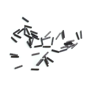
CVD Diamond Dressing Tools for Precision Applications
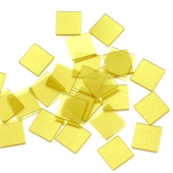
CVD Diamond for Thermal Management Applications
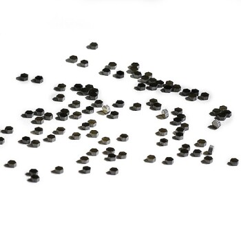
CVD Diamond Wire Drawing Die Blanks for Precision Applications
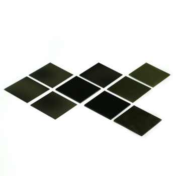
CVD Diamond Cutting Tool Blanks for Precision Machining
